2D semiconductors
The development of semiconductors lies in the heart of information industry. Increasing demand for computation ability nowadays requires highly integrated chips of conventional semiconductor devices with decreasing size which has, however, reached the quantum limit (Moore’s law). The newly discovered atomically thin 2D semiconductors retain intrinsic properties of their 3D bulk counterparts and are thus highly promising to bypass the traditional limit because of the following reasons: (1) They need smaller channel length than the conventional Si-based chips. (2) Their carrier densities are highly tunable by various gating techniques. (3) Some of them show high mobility which allows fabrication of high-speed devices. (4) They can be stacked together with other 2D materials to make van der Waals heterostructures that exhibit a variety of intriguing properties such as electron correlations, magnetism, and topology.
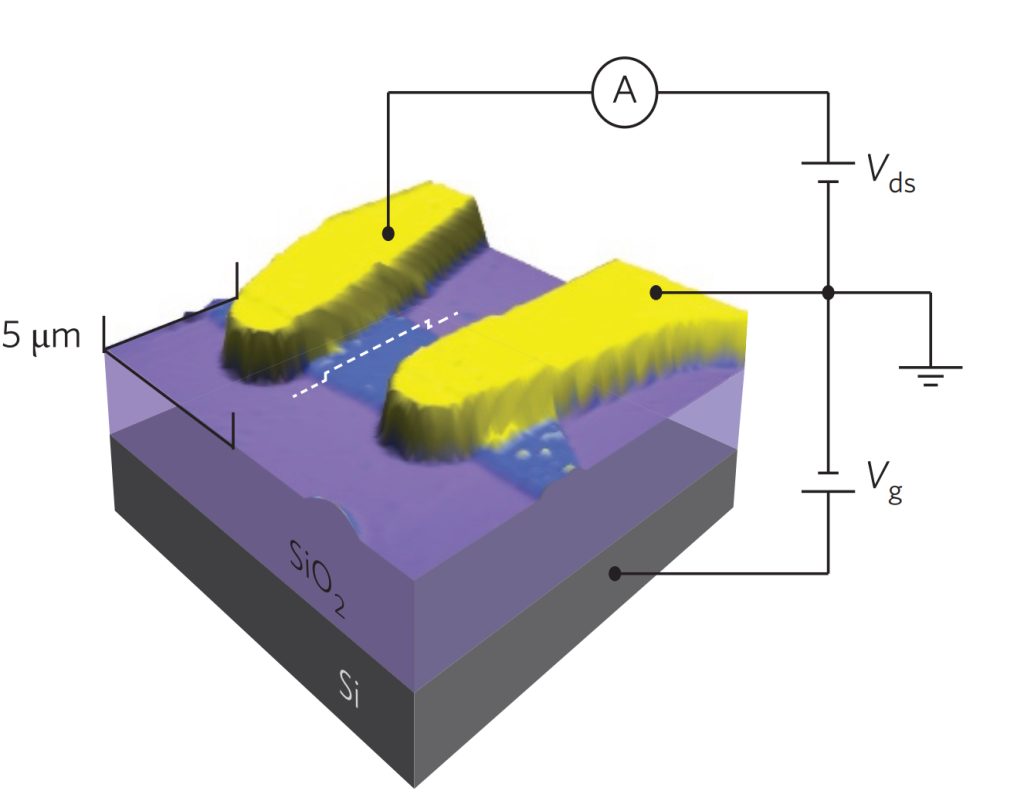
Graphene, a 2D semimetal, and black phosphorus (BP), a 2D semiconductor, have great potential in such device applications. We are interested in fabricating prototype field effect transistors from these materials and characterizing them by quantum transport measurement under low temperature and high magnetic field. Using the standard nanofabrication technique, we made for the first time few-layer BP field effect transistors with high on-off ratio, high mobility, and well-define current saturation (Nature nanotechnology 10 372-377 (2014)). Using the dry transfer technique, we fabricated BP high mobility devices (Nature nanotechnology 11, 593-597 (2016)) and graphene moiré superlattices devices (Nano Letters 17, 3576-3581(2017)), in which novel integer quantum Hall effect was observed.
A controllable growth method of high-quality 2D semiconductor wafers is crucial for their industrial application. We are also interested in developing the growth method (e.g., chemical vapor deposition and molecular beam epitaxy) as well as home-built equipment to achieve this goal.